- 您现在的位置:买卖IC网 > Sheet目录1905 > ATMEGA649V-8MI (Atmel)IC AVR MCU FLASH 64K 1.8V 64QFN
3
2552K–AVR–04/11
ATmega329/3290/649/6490
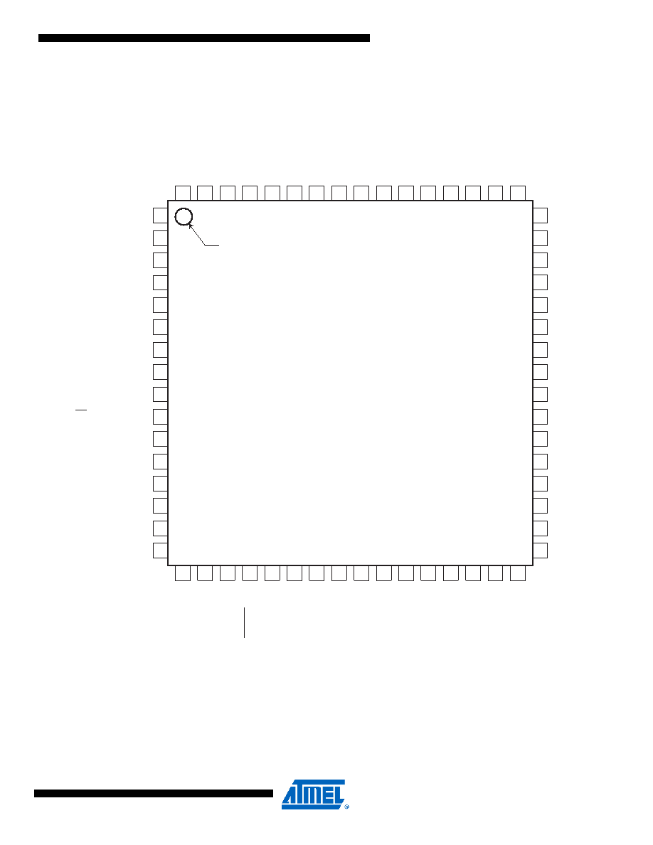
Figure 1-2.
Pinout ATmega329/649
Note:
The large center pad underneath the QFN/MLF packages is made of metal and internally con-
nected to GND. It should be soldered or glued to the board to ensure good mechanical stability. If
the center pad is left unconnected, the package might loosen from the board.
PC0 (SEG12)
V
CC
GND
PF0
(ADC0)
PF7
(ADC7/TDI)
PF1
(ADC1)
PF2
(ADC2)
PF3
(ADC3)
PF4
(ADC4/TCK)
PF5
(ADC5/TMS)
PF6
(ADC6/TDO)
AREF
GND
A
V
CC
17
61
60
18
59
20
58
19
21
57
22
56
23
55
24
54
25
53
26
52
27
51
29
28
50
49
32
31
30
(RXD/PCINT0) PE0
(TXD/PCINT1) PE1
LCDCAP
(XCK/AIN0/PCINT2) PE2
(AIN1/PCINT3) PE3
(USCK/SCL/PCINT4) PE4
(DI/SDA/PCINT5) PE5
(DO/PCINT6) PE6
(CLKO/PCINT7) PE7
(SCK/PCINT9) PB1
(MOSI/PCINT10) PB2
(MISO/PCINT11) PB3
(OC0A/PCINT12) PB4
(OC2A/PCINT15)
PB7
(T1/SEG24)
PG3
(OC1B/PCINT14) PB6
(T0/SEG23)
PG4
(OC1A/PCINT13) PB5
PC1 (SEG11)
PG0 (SEG14)
(SEG15)
PD7
PC2 (SEG10)
PC3 (SEG9)
PC4 (SEG8)
PC5 (SEG7)
PC6 (SEG6)
PC7 (SEG5)
PA7 (SEG3)
PG2 (SEG4)
PA6 (SEG2)
PA5 (SEG1)
PA4 (SEG0)
PA3 (COM3)
PA0
(COM0)
PA1
(COM1)
PA2
(COM2)
PG1 (SEG13)
(SEG16)
PD6
(SEG17)
PD5
(SEG18)
PD4
(SEG19)
PD3
(SEG20)
PD2
(INT0/SEG21)
PD1
(ICP1/SEG22)
PD0
(TOSC1)
XTAL1
(TOSC2)
XTAL2
RESET/PG5
GND
V
CC
INDEX CORNER
(SS/PCINT8) PB0
2
3
1
4
5
6
7
8
9
10
11
12
13
14
16
15
64
63
62
47
46
48
45
44
43
42
41
40
39
38
37
36
35
33
34
ATmega329/649
发布紧急采购,3分钟左右您将得到回复。
相关PDF资料
ATMEGA8515L-8JUR
MCU AVR 8KB FLASH 8MHZ 44PLCC
ATMEGA8515L-8PJ
IC MCU AVR 8K 5V 8MHZ 40-DIP
ATMEGA8535-16JUR
MCU AVR 8K FLASH 16MHZ 44PLCC
ATMEGA8535L-8PJ
IC MCU AVR 8K 5V 8MHZ 40-DIP
ATMEGA88-15MT2
MCU AVR 8K FLASH 15MHZ 32-QFN
ATMEGA88-20AUR
MCU AVR 8K FLASH 20MHZ 32TQFP
ATMEGA88P-20AUR
MCU AVR 8KB FLASH 20MHZ 32TQFP
ATMEGA8HVA-4CKU
MCU AVR 8K FLASH 4MHZ 36-LGA
相关代理商/技术参数
ATmega649V-8MU
功能描述:8位微控制器 -MCU AVR 64K FLASH 2K EE 4K SRAM ADC LCD RoHS:否 制造商:Silicon Labs 核心:8051 处理器系列:C8051F39x 数据总线宽度:8 bit 最大时钟频率:50 MHz 程序存储器大小:16 KB 数据 RAM 大小:1 KB 片上 ADC:Yes 工作电源电压:1.8 V to 3.6 V 工作温度范围:- 40 C to + 105 C 封装 / 箱体:QFN-20 安装风格:SMD/SMT
ATMEGA649V-8MUR
功能描述:8位微控制器 -MCU AVR 64KB FLSH 2KB EE 4KB SRAM LCD8MHz1.8V RoHS:否 制造商:Silicon Labs 核心:8051 处理器系列:C8051F39x 数据总线宽度:8 bit 最大时钟频率:50 MHz 程序存储器大小:16 KB 数据 RAM 大小:1 KB 片上 ADC:Yes 工作电源电压:1.8 V to 3.6 V 工作温度范围:- 40 C to + 105 C 封装 / 箱体:QFN-20 安装风格:SMD/SMT
ATMEGA64A-AN
功能描述:8位微控制器 -MCU 16MHz 105C RoHS:否 制造商:Silicon Labs 核心:8051 处理器系列:C8051F39x 数据总线宽度:8 bit 最大时钟频率:50 MHz 程序存储器大小:16 KB 数据 RAM 大小:1 KB 片上 ADC:Yes 工作电源电压:1.8 V to 3.6 V 工作温度范围:- 40 C to + 105 C 封装 / 箱体:QFN-20 安装风格:SMD/SMT
ATMEGA64A-ANR
功能描述:8位微控制器 -MCU 16MHz 105C RoHS:否 制造商:Silicon Labs 核心:8051 处理器系列:C8051F39x 数据总线宽度:8 bit 最大时钟频率:50 MHz 程序存储器大小:16 KB 数据 RAM 大小:1 KB 片上 ADC:Yes 工作电源电压:1.8 V to 3.6 V 工作温度范围:- 40 C to + 105 C 封装 / 箱体:QFN-20 安装风格:SMD/SMT
ATMEGA64A-AU
功能描述:8位微控制器 -MCU 64K Flsh 2K EEPROM 4K SRAM 16MHz RoHS:否 制造商:Silicon Labs 核心:8051 处理器系列:C8051F39x 数据总线宽度:8 bit 最大时钟频率:50 MHz 程序存储器大小:16 KB 数据 RAM 大小:1 KB 片上 ADC:Yes 工作电源电压:1.8 V to 3.6 V 工作温度范围:- 40 C to + 105 C 封装 / 箱体:QFN-20 安装风格:SMD/SMT
ATMEGA64A-AUR
功能描述:8位微控制器 -MCU AVR 64KB FLSH 2KB EE 4KB SRAM-16MHz IND RoHS:否 制造商:Silicon Labs 核心:8051 处理器系列:C8051F39x 数据总线宽度:8 bit 最大时钟频率:50 MHz 程序存储器大小:16 KB 数据 RAM 大小:1 KB 片上 ADC:Yes 工作电源电压:1.8 V to 3.6 V 工作温度范围:- 40 C to + 105 C 封装 / 箱体:QFN-20 安装风格:SMD/SMT
ATMEGA64A-MN
功能描述:8位微控制器 -MCU 16MHz MLF 105C RoHS:否 制造商:Silicon Labs 核心:8051 处理器系列:C8051F39x 数据总线宽度:8 bit 最大时钟频率:50 MHz 程序存储器大小:16 KB 数据 RAM 大小:1 KB 片上 ADC:Yes 工作电源电压:1.8 V to 3.6 V 工作温度范围:- 40 C to + 105 C 封装 / 箱体:QFN-20 安装风格:SMD/SMT
ATMEGA64A-MNR
功能描述:8位微控制器 -MCU 16MHz MLF105C RoHS:否 制造商:Silicon Labs 核心:8051 处理器系列:C8051F39x 数据总线宽度:8 bit 最大时钟频率:50 MHz 程序存储器大小:16 KB 数据 RAM 大小:1 KB 片上 ADC:Yes 工作电源电压:1.8 V to 3.6 V 工作温度范围:- 40 C to + 105 C 封装 / 箱体:QFN-20 安装风格:SMD/SMT